-
-
THE M.I.T. 1978
VLSI SYSTEM DESIGN COURSE
by
Lynn Conway
Copyright @ 2000-2007, Lynn Conway.
All Rights Reserved
[V 9-19-11]
Printable
PDF version
-
- This course was an important milestone in the development,
demonstration and evaluation of the Mead-Conway structured VLSI design
methods. Lynn Conway conceptualized and planned the course during the late
spring and summer of '78, and taught the course while serving as Visiting
Associate Professor of EECS at MIT in the fall of '78 and early '79.
-
- The textbook for the course was a nearly-completed draft of
"Introduction to VLSI Systems" by Mead and Conway. The text was being
written and edited at the time using the Alto computers at Xerox PARC.
Copies of the draft text were printed up for all course participants using
the laser printers at PARC (with color plates reproduced on new color
copiers there). In addition to the textbook,
Lynn developed very detailed lecture
notes for this course, and taken together all these materials provided a
comprehensive plan for such courses. Lynn compiled these materials into an "Instructors'
Guidebook", and that guidebook was later used to implement similar
courses by faculty members at many
other universities during the following several years.
-
- This new form of course was aimed at EECS seniors and grad students. The
goal was for them to learn all basics of VLSI system design in half a
semester, then do a real design during the rest of the semester using the
very basic computer-based tools available at the time (a text-based graphics
language and HP pen-plotters). Design files were then to be transmitted via
Arpanet to Xerox PARC, merged into a multi-project chip file, and
implemented at Micromask and HP via QTA mask and fab. The packaged, bonded
chips were to be available about a month after the conclusion of the course.
-
-
Professor Jonathan Allen
of M.I.T.'s EECS Department and Research Laboratory of Electronics served as
host and faculty coordinator for this intensive laboratory based course. Jon
played a key role in helping establish the course environment and in helping
Lynn negotiate the logistics of running a new, experimental course at the
Institute. Prof. Allen himself later went on to teach VLSI design courses at
M.I.T. One of Prof. Allen's Ph.D. students (Glen Miranker) served as
graduate teaching assistant for the course, and played an important role in
getting the design lab up and running so that students could layout and
implement their projects.
-
- When this experimental prototype course worked-out completely as planned,
it was a
demonstration-proof of the validity and potential of the new Mead-Conway
VLSI system design methods . Prior to this time, complex digital chip
designs required a team of "architects, logic designers, circuit designers,
circuit layout designers, and process experts", and took many months to a
year to complete. Some of the projects completed in this course set entirely
new standards for length of time from conceptualization to implementation,
given their complexity, bringing wide notice to the course as a result. Guy
Steele's LISP microprocessor, in particular, greatly excited and challenged
other architects and designers who heard about it (see project 17, below);
Guy's project undoubtedly triggered the participation of a number of key
system architects at Stanford and Berkeley in the later MPC79 and MPC580
efforts in '79 and '80.
This course also played a key role in
the evolution, development and demonstration of new rapid-turnaround chip
prototyping methods - methods later documented in the "A
Guidebook to LSI Implementation" edited by Bob Hon and Carlo Sequin. The
opportunistic use of the Arpanet for interaction with the "foundry" at Xerox
PARC and HP in Palo Alto, CA, provided key experiences that led to innovation in
1979 of the network-server, multi-university chip prototyping infrastructure
deployed and demonstrated as part of "MPC79". The success of MPC79 led
to the transfer of that infrastructure to USC-ISI, where it
became known as the "MOSIS" service. MOSIS has been operated as a national
infrastructure for rapid chip prototyping for university researchers and
students since 1981, with support from DARPA and later from NSF.
This document includes a list of participants in the
course, photos of various course activities, and a detailed course plan
(from the "Instructors Guide to VLSI Design", produced as a byproduct of the
course). You'll also find information about this course at the MIT
Research Laboratory of Electronics (RLE)
Circuits and Systems Group history site.
-
-
-
Page Contents:
- 1. Class Photo
- 2. List of
participants
- 3. Photos from the
course
- 4. The MIT '78 VLSI
System Design Course: A guide for the Instructor
of VLSI Design
-
[ Includes
links to PDF's of lecture notes;
see this link to access the complete document
]
-
Table of Contents
-
The
Plan: Course Abstract, Goals,
Outline, Student
Projects, Tools
-
The
Result:
Letter to participants,
List of Projects,
Implementation Sequence
- 5. MIT '78
Multiproject Chip Map
- 6. MIT '78
Multiproject Chip Photo
- 7. Example Project
Wire-Bonding Map
-
-
-
-
-
-
-
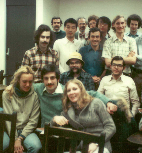
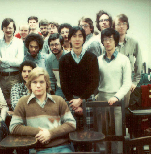
1.
Class Photo:
-
Students and faculty observers, MIT'78 VLSI design course
-
[Note: Not all participants were in this photo; name ID chart
will be compiled soon]
|
 |
 |
-
-
- 2.
Course participants:
-
-
-
-
-
-
-
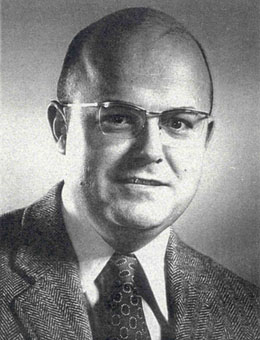 |
- Prof.
Jonathan Allen
- [1934-2000]
-
- Jon Allen was the MIT faculty member who coordinated
Lynn's visit and supported her new course at MIT. Jon played a
key role in insuring the success of the course. He and went on
to do research in VLSI systems and teach the course himself in
following years.
|
-
-
-
-
- 3. Photos from the
course:
-
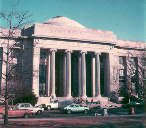
-
- MIT in 1978
-
-
-
-
- RLE Building: Site of Lynn's office and VLSI design lab
-

-
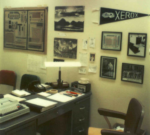
Lynn’s office at MIT:
Lynn used the TI terminal (lower-left) to communicate via
the Arpanet to Xerox PARC.
-
-
-
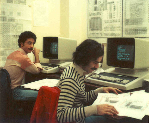
The design
lab:
Designs were entered directly in CIF and check-plotted on
an HP pen-plotter
-
-
-
-
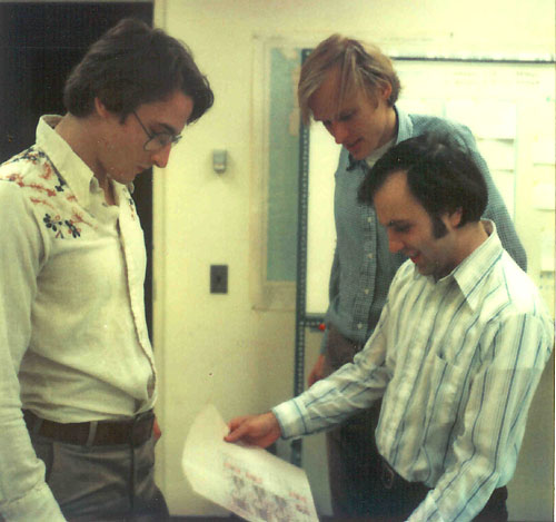
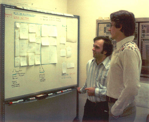
- Jim Cherry, Gerald Roylance and Glen Miranker
checking a design plot
-
-
-
Status checking
before final merge
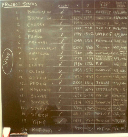
-
- Glen Miranker and Jim Cherry check out the
status of the MIT multi-project chip area planning,
- using our "high-tech" space allocation system
(scaled pieces of paper).
-
-
-
-
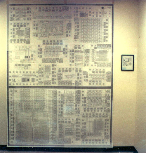
- The final sanity check before maskmaking:
- A wall-sized overall check plot made at Xerox
PARC from Arpanet-transmitted design files,
- showing the student design projects merged
into multiproject chip set.
-
-
-
-
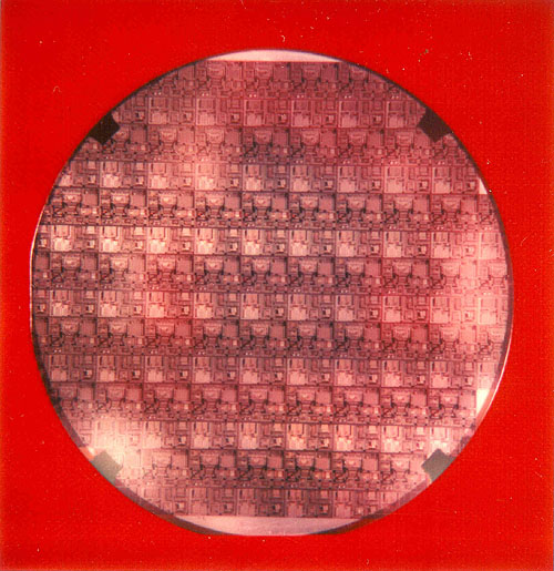
- One of the wafers just off the HP fab line
containing the MIT'78 VLSI design projects:
- Wafers were then diced into chips, and the
chips packaged and wire bonded
- to specific projects, which were then tested
back at M.I.T.
-
-
-
-
-
-
-
4. Excerpts
from Lynn's "Instructors Guide"
of
all lecture notes and handouts from this course
[Includes links to PDF's of
lecture notes and handouts; see this
link for the complete document]
-
- The MIT'78 VLSI System Design Course:
- A Guidebook for the Instructor of VLSI System Design
-
- Lynn Conway
- Manager, LSI Systems Area, Xerox PARC, and
Visiting Assoc. Prof. of
Electrical Engineering & Computer Science, M.I.T., 1978-79.
-
-
- In the fall of 1978, a course entitled "Introduction to VLSI Systems" was
offered by M.I.T.'s Department of Electrical Engineering and Computer
Science. This document is a compendium of information concerning that
course. It is intended to serve as a basic guidebook for instructors
preparing similar courses.
-
-
- [ Filed on: <Conway>M1Tguide.VLSI, August 12, 1979 5:55
PM
Copyright © 1979, Lynn Conway. All
Rights Reserved.
-
-
-
-
- TABLE OF CONTENTS:
-
- I. The Plan:
-
- > Abstract of the course.
> Goals of the course, relevant student
backgrounds and interests, and required prerequisites.
> A detailed
outline of the course (with links to the detailed lecture notes for each
lecture).
> Discussion of the sort of class projects required.
> Design tools and procedures required for class project implementation.
-
- II. The Result:
-
- > Letter to the participants, indicating the status of the projects.
>
List of the student LSI projects.
> List of the participating
organizations and schedule for chip set implementation.
> Map of the
MIT. '78 multiproject chip set.
> Photomicrograph of the MIT. '78
multiproject chip set.
-
- III. Lecture Notes:
-
- > A complete set of notes for the seventeen formal lectures and for the
various other class meetings of the MIT. course (see the detailed Outline in
part 1). The notes were handwritten out in detail, this being the
instructor's method of lecture preparation. Note that a few figures were in
color in the original notes; hopefully the reader will be able to deduce the
correct colors for these figures.
-
- IV. Homework and Project Assignments:
-
- > Homework was assigned only during the first half of the course, before
the project activities began. The homework emphasized material and
experiences useful as background for planning and working on projects.
Specific project assignments were given to keep the students on schedule
during the short, intensive project phase of the course.
-
- V. Other Course Handouts:
-
- > Student Background Questionnaire; other questionnaires.
> CIFtran
User's Guides.
> Examples of the Wire-Bonding Maps returned to students with their
packaged chips.
-
-
-
- I. The Plan:
Massachusetts Institute of Technology
Department of Electrical Engineering and Computer Science
-
- Special Subject in Electrical Engineering and Computer Science:
6.978: Introduction to VLSI Systems (A) (New)
-
- Prereq.: Limited Enrollment; permission of the instructor required.
Year: G(1)
3-3-6
-
- An introduction to the design and implementation of very large scale
integrated systems. The course provides sufficient basic information about
integrated devices, circuits, digital subsystems, and system architecture,
to enable the student to span the range of abstractions from the underlying
physics to complete VLSI computer systems. The course presents basic
procedures for designing and implementing digital integrated systems,
including a structured design methodology, use of stick diagramming, use of
a scalable set of ratioed design rules, use of a symbolic layout language,
techniques for the estimating delay times, and use of a starting frame of
layout artifacts for organizing multi-project chip sets and conveying them
thru implementation. The course also examines the effects of scaling down
the dimensions of devices and systems, as will occur with future
improvements in fabrication technology.
-
- After developing this overall context, the course examines the
interdependance of integrated system architecture, design methodology, and
the procedures used for patterning, fabrication, and testing. Techniques for
simplifying, systematizing, and reducing the time involved in integrated
system design and implementation will be discussed.
-
- The subject matter will be reinforced by actual experience in LSI design:
students will complete, through layout, the design of digital subsystem
projects containing on the order of several hundred to perhaps several
thousand transistors. NMOS will be used as the technology for course
examples and projects. Selected student projects will be organized into a
multi-project chip set to be implemented by commercial mask and fab firms.
-
- L. A. Conway
-
- Tuesday and Thursday, 1:30- 3:00
-
-
-
6.978: Introduction to VLSI Systems
-
- Goals of the Course, Relevant Student Backgrounds, and Prerequisites
- Required for this Course:
-
- This is an interdisciplinary course and is likely to be taken by students
from a wide range of backgrounds, including CS students primarily interested
in computer architecture and system design methodology, and EE students
primarily interested in solid state physics and integrated circuit design.
The goals of the course are:
-
- (i) for CS students and those interested in computer architecture:
to take the mystery out of integrated circuit and system design, explore
some of the many CS issues involved in integrated system architecture and
design methodology, and indicate the exciting possibilities ahead for the
expansion of computing power by VLSI systems.
-
- (ii) for EE students and those interested in device physics and
integrated circuit design: to get a feeling for the nature of the chips that
will be designed in the future, take some of the mystery out of the design
of complex integrated digital systems, and illustrate the additional
opportunities for optimization at the system level as opposed to the device
and circuit layout level.
-
- (iii) for all participants: to outline the many opportunities now
present for major advancements in the state of the art by collaborative
efforts involving applied physicists, electrical engineers, computer
architects, and computer scientists.
-
- (iv) to develop and debug a set of basic tools and procedures for enabling
the design and implementation of LSI multi-project chip sets at M.I.T.
-
- Ideally, students will have taken the following prerequisite courses, or
have the equivalent background experience: Introductory Network Theory
(6.011), Electronic Devices and Circuits (6.012), Structure and
Interpretation of Computer Languages (6.031), Computation Structures
(6.032), Switching Circuits, Logic and Digital Design (6.082), Digital
Systems Project Laboratory (6.112). However, those lacking the required
prerequisites (including recommended undergraduates) may take the course
with the permission of the instructor.
-
- 6.978: Course textbook
-
- Carver Mead and Lynn Conway, Introduction to VLSI Systems, July 1978; a
pre-publication limited printing of a textbook in preparation; distributed
to course participants. This textbook will be published by Addison-Wesley
Publishing Co., Reading, Massachusetts, in the fall of 1979.
-
-
-
- 6.978: Introduction to VLSI Systems:
-
- Course Outline: [The final outline of the actual
course.]
-
-
- Week #1:
-
- Sept. 12: Lecture #1
Administrative Details.
Course Overview.
MOS as an Abstract technology.
- Patterned conducting layers separated by insulating material.
Color coding, Switches, Simple logic structures, Some examples.
-
- Homework #1 (part 1) (Due 19th):
Stick diagram several functions.
-
- Sept. 14: Lecture #2
The MOS transistor.
Dimensions, basic function, transit times, current/voltage characteristics.
- The basic inverter.
Structure, function, transfer characteristics, logic threshold voltage, intro.
to delays.
NAND and NOR logic circuits.
-
- Homework #1 (part 2) (Due 19th):
Logic gate vs switch-logic designs for selector.
-
- Reading Assignment.-
Ch.l: Intro., MOS Transistor, Basic Inverter, Inverter Delay, Basic NAND and
NOR Logic Circuits.
Ch.2: Intro.
Ch.3: Intro., Notation, Combinational Logic.
-
-
- Week #2:
-
- Sept. 19: Lecture #3
More on delays.
Transit time and inverter pair delay.
Notation.
Two phase clocks.
The shift register.
Shift register arrays.
Relating Different Levels of Abstraction .
Implementing Dynamic Registers.
Implementing a Stack: the basic cell.
-
- Homework #2 (Due 26th):
More stick diagram-level designs (two-dimensional stack, several PLA
examples).
-
- Sept. 21: Lecture #4
Stack subsystem design, control timing, generation of control signals.
Register to Register Transfer.
Combinational Logic.
The Programmable Logic Array.
- Basic concept, Circuit design, and stick diagram of example.
- Finite State Machines,
- Basic concept, use of PLA form of, symbolic and encoded transition tables,
traffic light controller example.
-
- Reading Assignment.-
Ch.3. Two-Phase Clocks, The Shift Register, Relating Different Levels of
Abstraction, Implementing Dynamic Registers, Designing a Subsystem, The
Programmable Logic Array, Finite State Machines.
-
- Week #3:
-
- Sept. 26: Lecture #5
Patterning.
The Silicon Gate n-Channel Process.
Design Rules, basis for and detailed description of.
-
- Homework #3 (Due 3rd):
Finite state machine example, from problem statement to encoded transition
table;
layout of compact shift register cell; layout of stack cell.
-
- Sept. 28: Lecture #6
Review the process, discuss some advantages of Silicon-Gate process over
earlier ones.
Explanation of sheet resistivity; estimating ratios and resistances from
layout geometries.
Layout ideas.
Current limitation in metal lines.
Go thru some layout examples: selector; shift register.
-
- Reading Assignment.-
Ch.2. Patterning, Silicon Gate n-Channel Process, Design Rules, Electrical
parameters, Current Limitations in Conductors.
Ch.4. Introduction.
-
-
- Week #4:
-
- Oct. 3: Lecture #7
Driving Large Capacitive Loads.
Space vs Time.
Super Buffers.
Body effect.
Depletion mode vs enhancement mode pullups.
-
- Homework #4 (Due 12th):
Stick diagram and layout of serial bit string comparator.
-
- Oct. 5 Lecture #8
Layout of the PLA.
Detailed description of an OM2 subsystem: the Barrel Shifter.
Description of function and structure of the serial bit string comparator (to
get people started on HW #4).
-
- Reading Assignment:
Ch.l. Driving large capacitive loads, super buffers.
Ch.4. Patterning and fabrication.
-
-
- Week #5: [Oct. 10 is vacation day]
-
- Oct. 12: Lecture #9
An overview of implementation.
Hand Layout and Digitization using a Symbolic Layout Language.
The Caltech Intermediate Form, detailed description of, including tutorial on
transformations.
-
- Description of the sorter subsystem (to get people started on HW #5).
Homework #5 (Due 17th):
Construct OF code for the OM register cell pair: the Sorter Problem
-
- Reading Assignment.,
Ch.4. Hand Layout and Digitization Using a Symbolic Layout Language, The
Caltech Intermediate Form.
-
- Project Assignment #1 (Due 26th) :
[The Lab opens this week (CIFtran now ready)].
Practice editing of text files, listing of text files, plotting of CIF-code
layout files on the HP color plotters;
Keyin and plot OF code for HW #5; Select course project and write a short
project proposal.
-
- Week #6:
-
- Oct. 17: Lecture #10
Discuss plan for remainder of course: what will be in the final project
assignment schedule to be handed out next week, planned seminar series, the
midterm, some rules of the game for projects.
Description of lab facilities, CIF software for editing/plotting of layouts.
Detailed discussion of the sorter subsystem problem.
-
- Homework #6 (Due 24th):
Construct stick diagram for the Sorter Problem.
-
- Oct. 19: Lecture #11
More on course schedule/project schedule, rules of the game, area estimates.
Yield statistics.
Delays in Another Form of Logic Circuitry,
Transit Times and Clock Periods.
-
- Reading Assignment:
Ch.l. Delays in another form of Logic Circuitry, Transit Times and Clock
Periods.
Ch.2. Yield Statistics.
-
-
- Week #7:
-
- Oct. 24: Lecture #12
Handout the Guide to LSI Implementation, discuss contents, suggest readings.
Discuss how class chip set will be implemented.
Describe cell library, particularly the PLA cells and Input/Output pads.
Detailed description of the multiproject. chip concept, starting frame, past
examples.
-
- Handout Project Assignments #2, #3, and #4:
#2 (Due Nov.9): Detailed project description.
#3 (Due Nov.21): Preliminary layout (a key item for determining chip set space
comittments).
#4 (Due Dec.12): Final project reports.
-
- Oct. 26: Lecture #13
More on implementation: Interacting with mask and fab firms.
- What happens when the wafers come back: electrical characterization,
packaging, functional testing.
- The Stored Program Computer, a tutorial on the basics:
Alternative control structures,
The stored program computer;
Fetch-execute sequence;
Microprogrammed control.
-
- Suggested reading.
During the next several weeks, read the first half of Chapter 5, and Chapter
6.
-
-
- Week #8:
-
- Oct. 31: Seminar
Interactive Graphic Aids for Integrated System Design.
Douglas Fairbairn, PARC
-
- Nov. 2: Midterm Exam
A two hour examination on the basics covered so far.
-
- Week #9:
-
- Nov. 7: Lecture #14
Discuss midterm examination.
Effects of Scaling Down the Dimensions of MOS Circuits and Systems.
Discuss the Scaling of Transit time, Electrical parameters, Current, Current
density, Power density.
-
- Nov. 9: Lecture #15
Summarize Scaling so far, introduce idea of switching energy and its scaling,
scaling of delays to outside world,
Sub-threshold conductance phenomenon, and scaling of
Discussion of limiting factors.
Project Assignment #2 Due Today.
-
-
- Week #10:
- Nov. 14: Lecture #16
Patterning and Fabrication in the Future:
Scaling of Patterning and Processing Technology, the Runout phenomenon, E-beam
and x-ray lithography;
The opportunity for remote-entry, fast-turnaround implementation of designs.
-
- Nov. 16: Lecture #17
Memory Cells and Subsystems:
Discussion of the relative area, power, delay, and overhead circuitry for a
variety of on-chip memory subsystems, including the shift register, the OM2
register cell, the 6-transistor static RAM, the 3-transistor dynamic RAM,
and the 1-transistor dynamic RAM.
-
-
- Week #11:
-
- Nov. 21: Seminar
- VLSI Implementation of Speech Processing Functions
Richard Lyon, PARC
-
- Project Assignment #3 Due Today.
Discussion of project status so far.
- Beginning to allocate space on the chip set.
- Update on the rules of the game.
Selected preliminary project design files will be transmitted to PARC this
week, for individual project plotting and checking at PARC, and to test the
overall data transmission scheme.
-
- [Nov. 23 is vacation day]
-
-
- Week #12:
-
- Nov. 28: Seminar
Electrical test patterns for electrical characterization and process
parameter extraction.
Rick Davies, PARC.
-
- Project update:
More information about status of space, map of the chip set, library cells;
- Q and A session to pin down final details.
-
- Nov. 30: Description of Selected Projects by Students in the class:
Four projects (from among those already selected for inclusion in the chip
set) will be selected for presentation to the class by their designers.
-
- Project update:
Discussion of the final status of projects, distribution of plots arriving
from PARC, discussion of various known bugs in the various software packages
and how to get around them, contingency plans, getting ready for the
upcoming design cutoff date, how to sign-off on your design file.
-
- Suggested readings:
Selected portions of Chapter 8.
-
- Week # 13:
-
- Dec. 5: Seminar
Highly Concurrent Systems.
Carver Mead, Caltech
- Projects.- Today is the design cutoff date, all project design files
must be at PARC for merging into the MPC tomorrow.
-
- Dec. 7: Seminar
Recursive Machines.- A non-von Neumann VLSI Architecture
Wayne Wilner, PARC
-
-
- Week # 14:
-
- Dec. 12: Final Meeting of Class
- Project Assignment #4 (Final Project Report) Due Today.
- Complete Course feedback questionnaire.
-
- Status of the projects: list of those that got on the chip set.
Multi-project chip set progress report: how the implementation is going.
Planned activities during IAP, after the wafers are returned.
Discussion of further reading references
- (take some class photos).
-
-
-
-
- 6.978: Introduction to VLSI Systems
-
- Student Projects:
-
- Much of this course's material, while basic, is new and is not yet part of
the academic EE/CS culture. Thus, a strictly lecture oriented course faces
tutorial obstacles, as the terminology, artifacts, and abstractions involved
will be completely new to most students. A solution is to orient the course
around hands-on LSI digital design projects. Actual design experience will
enable students to quickly visualize the overall context of the course.
-
- Early in the course, students will define and begin work on LSI projects
on the order of useful digital subsystems based on a single cell design,
such as a stack, FIFO, etc. Alternatively, the student might design a simple
finite state machine controlling a very simple data structure; the traffic
light controller in the text is the sort of thing I have in mind here, but
with a bit more than just the PLA itself implemented in LSI. By doing these
designs top-down, under time pressure, learning the material as they
proceed, with homework each week oriented around the projects to keep
everyone on schedule, the students will master the material. Students having
the listed prerequisites should be able to complete their projects in the
available time. Those who have completed what appear to be workable projects
by an early December multi-project chip design cutoff date will have the
added satisfaction of seeing their projects implemented. All students must
complete their projects thru checkplot of full layout by December 12.
-
- In addition to these projects, students having strong software backgrounds
might volunteer to also participate in group projects to provide software
support for the editing, plotting, and implementation of the LSI design
projects. Similarly, students having strong device physics and integrated
circuit backgrounds might volunteer to participate in a group project to
provide circuit simulation support for the LSI design projects. Other
volunteers from the class will be sought for participation in the merging
and management of the class project chip set.
-
-
-
-
- 6.978: Introduction to VLSI Systems
-
- Required Tools and Procedures for Student Project Implementation:
-
- The completion of digital subsystem projects, through at least layout,
will be an essential part of the course experience for most of the students.
Work on these projects will proceed at a rapid pace from the beginning of
the course thru mid-November, at which time selected completed projects will
be merged for implementation. The remaining project layouts may undergo
iteration till the end of the course.
-
- For all this to really be feasible requires certain software facilities
and some sort of graphics plotter. There must be software, and computing
facilities accessible to all students, for the input and editing of symbolic
layout descriptions and their subsequent interpretation to generate CIF
files. Ideally the layout descriptions would be given in a language such as
ICL. Alternatively, the descriptions could be given directly in CIF. There
must be a plotter, software for conversion of CIF files to plotter format,
and software to interface/support the plotter. A rather simple subset of
CIF2.0, supporting boxes at right angles and symbol definitions and calls,
would be adequate for the above.
-
- I will provide a complete and documented starting frame targeted for
several alternative mask and fab firms. The starting frame will be specified
in the simple subset of CIF2.0, and will contain several alternative
alignment marks, mask level codes, fiducial marks if required, scribe lines
of appropriate profiles, line width testers, test transistors, and,
possibly, electrical test patterns for sheet resistivity and line widths. A
documented set of input pads with lightning arrestors and output pads with
drivers, also in the CIF2.0 subset, will be provided for student use. This
starting frame, along with the above facilities, will enable the forming of
a multi-project chip set file for transmission to Xerox PARC via the
ARPANET. [ The ARPANET will thus be used by M.I.T. and Xerox PARC, both of
which are ARPA contractors, to demonstrate the feasibility of remote
submission of student LSI projects to a fast turnaround implementation
facility ]. This will be scheduled for early December. Final plots of the
chip set will then be done at PARC from the CIF file, to verify successful
composition and transmission. The CIF to PG conversion will be done at PARC,
and software blowbacks generated for final checking of the PG files. The
chip set will be implemented by silicon valley mask and fab firms. Wafers
will be fabricated and shipped back to M.I.T. by about mid-January. During
the latter part of the independent activities program, the wafers will be
electrically tested and then diced into chips, and the chips then mounted,
wire bonded, and functionally tested.
-
-
-
-
- II. The Result:
-
-
- Xerox Palo Alto Research Center
3333 Coyote Hill Road
Palo Alto, CA 94304
March 31, 1979
-
-
- To the students, staff, and faculty
participants in the fall semester '78
VLSI system design course at M.I.T.
-
- Dear Friends,
-
- The color photos of the 1978 M.I.T. multi-project chip set have arrived!
I'm sending one out to each of you. Enclosed with each photograph is a
detailed list of the class projects, and a map to help you locate specific
projects in the photograph.
-
- Quite a few people have had a chance to test their projects. So far, the
results are really very good, especially when considering the limited tools
we used and the time pressure all of us worked under: I have reports that
projects 3, 4, and 5 work completely correctly; project 6 has been partially
tested, and works correctly so far; the important subsections of project 7
work correctly; project 12 works completely correctly except for a couple of
inverted outputs; project 17 has some wiring bugs, but may be partially
testable, and I hear rumors that a bigger and better version is planned! I'd
appreciate hearing about any additional functional test results as they
become available.
-
- If in the future any of you undertake research or development activities
related to integrated systems, I'd be very interested in staying informed of
your work. Also, if you ever travel through the San Francisco Bay Area, and
have some time, plan to stop by and visit at PARC. Good luck to you all.
-
- Sincerely,
-
-
- Lynn Conway
-
-
-
-
-
-
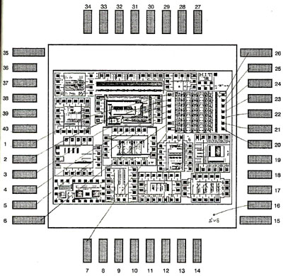
- M.I.T. 1978 Multi-project Chip Set:
-
- List of projects (see attached map and color copy of photo):
Filed on <Conway>maplist.memo
-
- 1. Sandra Azoury, N. Lynn Bowen Jorge Rubenstein:
Charge flow transistors (moisture sensors) integrated into digital subsystem
for testing.
- 2. Andy Boughton, J. Dean Brock, Randy Bryant,
Clement Leung: Serial data manipulator subsystem for searching and sorting
data base operations.
- 3. Jim Cherry: Graphics memory subsystem for
mirroring/rotating image data.
- 4. Mike Coln: Switched capacitor, serial
quantizing D/A converter.
- 5. Steve Frank: Writeable PLA project, based on
the 3-transistor ram cell.
- 6. Jim Frankel: Data path portion of a bit-slice
microprocessor.
- 7. Nelson Goldikener, Scott Westbrook: Electrical
test patterns for chip set.
- 8. Tak Hiratsuka: Subsystem for data base
operations.
- 9. Siu Ho Lam: Autocorrelator subsystem.
- 10. Dave Levitt: Synchronously timed FIFO.
- 11. Craig Olson: Bus interface for 7-segment
display data.
- 12. Dave Otten: Bus interfaceable real time
clock/calendar.
- 13. Ernesto Perea: 4-Bit slice microprogram
sequencer.
- 14. Gerald Roylance: LRU virtual memory paging
subsystem.
- 15. Dave Shaver Multi-function smart memory.
- 16. Alan Snyder Associative memory.
- 17. Guy Steele: LISP microprocessor (LISP
expression evaluator and associated memory manager; operates directly on
LISP expressions stored in memory).
- 18. Richard Stern: Finite impulse response digital
filter.
- 19. Runchan Yang: Armstrong type bubble sorting
memory.
- The following projects were
completed but not quite in time for inclusion in the project set:
- 20. Sandra Azoury, N. Lynn Bowen, Jorge
Rubenstein: In addition to project 1 above, this team completed a CRT
controller project.
- 21. Martin Fraeman: Programmable interval clock.
- 22. Bob Baldwin: LCS net nametable project.
- 23. Moshe Bain: Programmable word generator.
- 24. Rae McLellan: Chaos net address matcher.
- 25. Robert Reynolds: Digital Subsystem to be used
with project 4.
-
-
-
-
- MIT. 1978 Multi-project Chip Set:
-
- Chip Set Implementation Sequence:
Filed on <Conway>impsched.memo
-
- Information Management: Xerox PARC;
Masks: Micro Mask; Wafer Fabrication: HP Deer Creek;
Packaging:
M.I.T.
- A. Individual project design files, encoded in
CIF2.0, were transmitted to Xerox PARC via the ARPANET during 5 and 6
December 1978.
- B. Files were converted from CIF2.0 to ICARUS
format, and merged at PARC into a starting frame using ICARUS, based on a
tentative space allocation pasted up at M.I.T. The overall design file was
then converted to Mann PG format.
- C. Maskmaking began at Micro Mask, Inc. ~12
December, using their electron beam maskmaking system.
- D. Maskmaking at Micro Mask was pipelined during
the next several weeks with wafer fabrication at Hewlett-Packard's Deer
Creek Research Lab.
- E. Wafers (total of 41) were fabricated by 8
January 1979.
- F. Initial electrical testing and packaging were
done in M.I.T.'s Materials Science Lab.
- G. Packaged chips, custom wire-bonded to
individual projects, were available to students for functional testing by 18
January 1979.
-
-
-
|
5. Map of the M.I.T. '78 Multi-project Chip
Set: |
 |
-
-
-
-
-
|
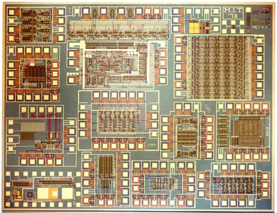
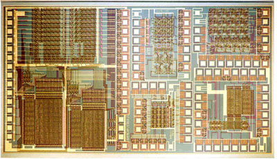
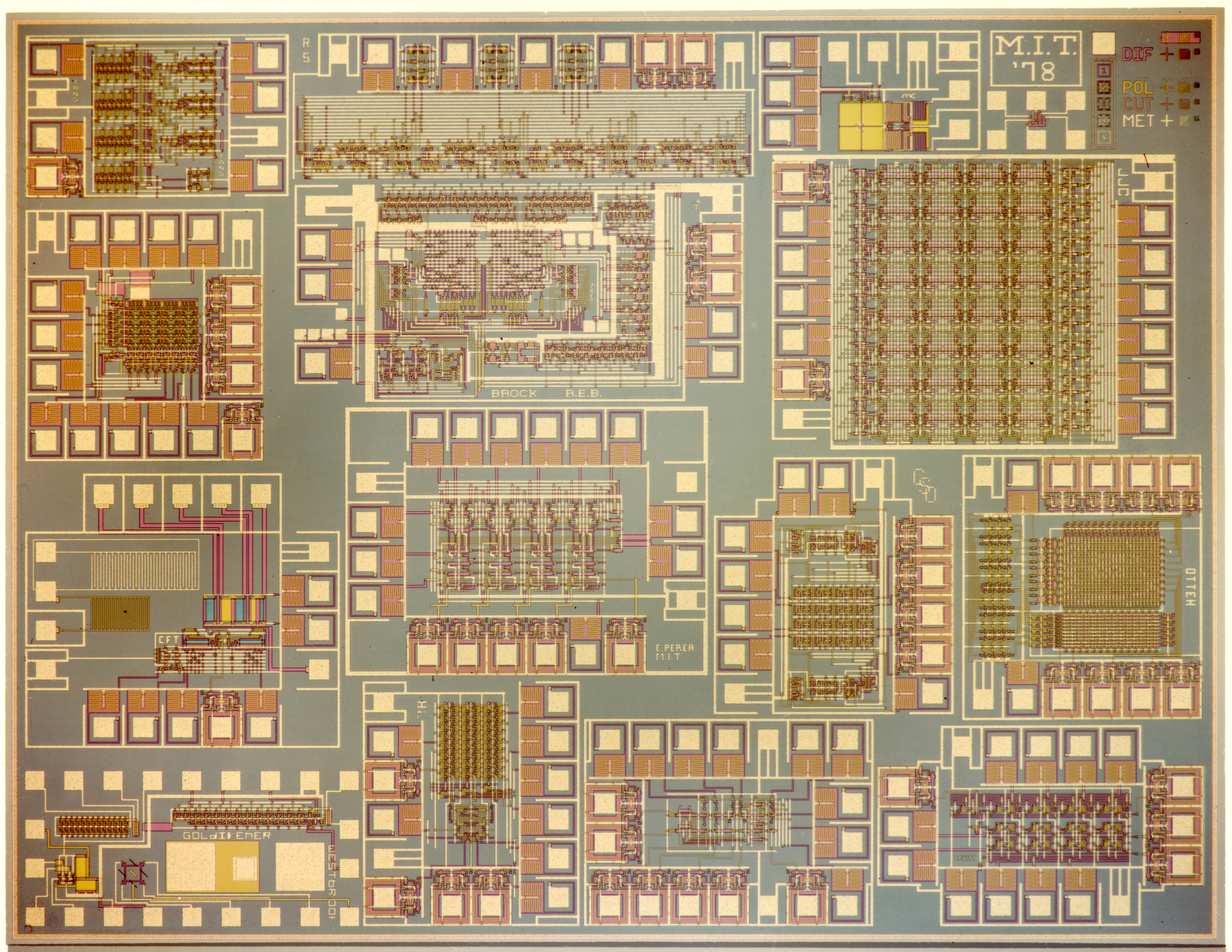
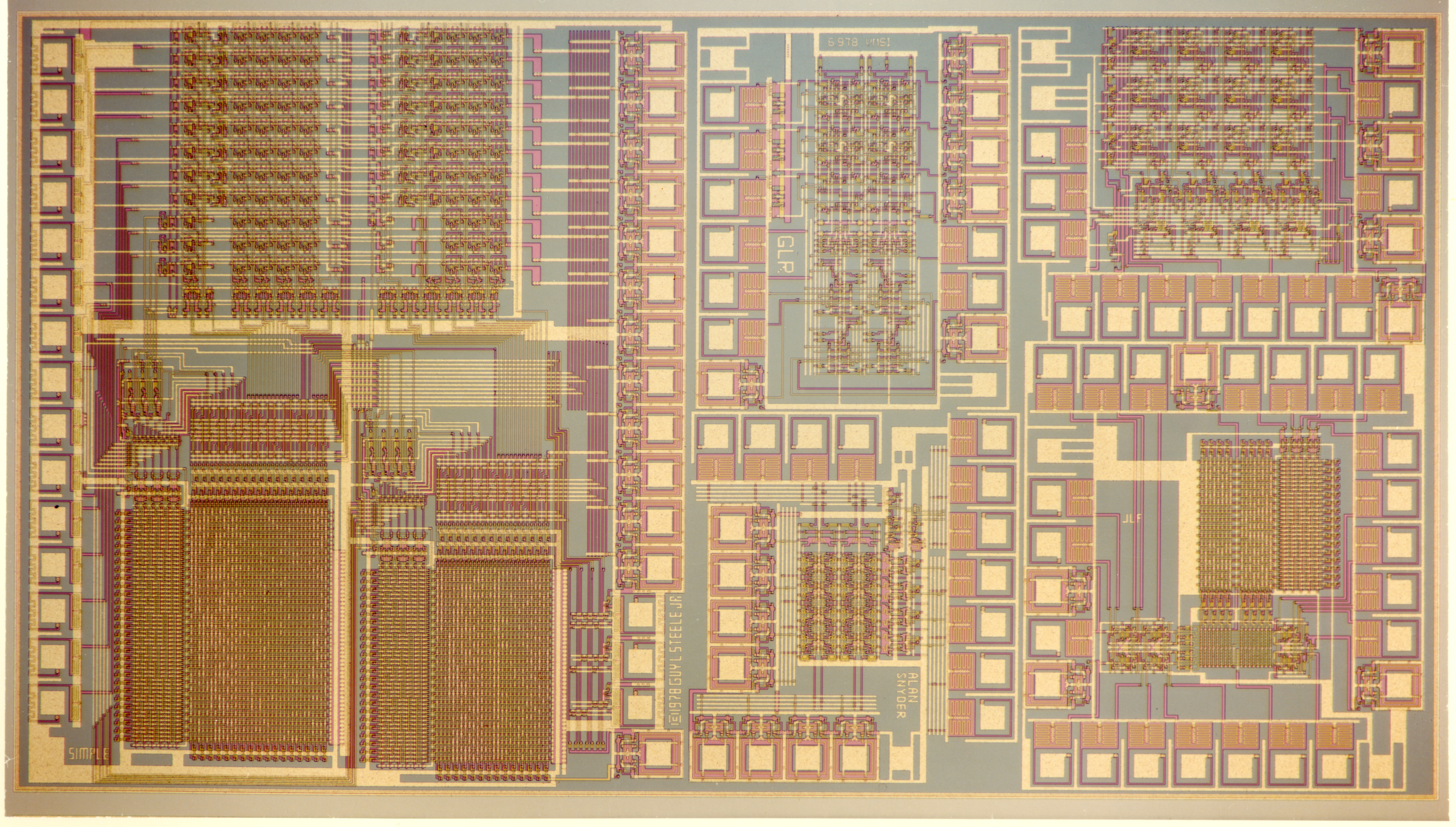
6. Photo of the
M.I.T. '78 Multi-project Chip Set: |
 |
 |
-
Link to a more detailed photo of the chip set.
Link to high-res photo of chip 1
(zoomable to 400%) (PDF, 2.0 mb)
Link to very high res JPG
of chip 1 (8.2mb)
Link to high-res photo of chip 2
(zoomable to 400%) (PDF, 1.4 mb)
Link to very high res JPG
of chip 2 (6.4 mb)
-
-
-
- 7. Example Project Wire-Bonding Map:
- [For Project #3, by Jim Cherry]
|
 |
-
LynnConway.com >
VLSI Archive > MIT'78 VLSI System
Design Course