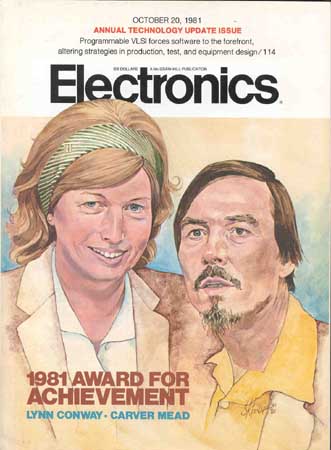
1981 Electronics AWARD FOR ACHIEVEMENT:
In 1981, Electronics awarded Carver Mead and Lynn Conway the magazine's annual Award for Achievement. Electronics was very widely read and highly regarded in the industry at the time. This award article sketches the story of the Mead-Conway work, and indicates the major impact their work was having within just 2 years of emerging from Xerox PARC and Caltech. The article follows:

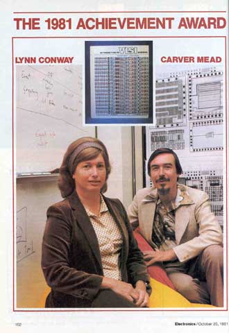
Electronics /October 20, 1981:
For optimal VLSI design efforts, Mead and Conway have fused device fabrication and system-level architecture
by Martin Marshall, Larry Waller, and Howard Wolff of the Electronics staff
The impact of Carver Mead and Lynn Conway on the design of very large-scale integrated circuits is bringing about a fundamental reassessment of how ICs are put together. Mead, the Caltech professor, and Conway, the Xerox system designer, have optimized the VLSI process by melding the concepts of fabrication at the device level and architecture at the system level to produce truly integrated systems.
The work they have done, individually and together, brought to fruition in their seminal textbook, "Introduction to VLSI Systems," is truly monumental. In the area of structured IC-design methodology, they not only have helped spawn a common design culture so necessary in the VLSI era, but they have greatly increased interaction between university and industry so as to stimulate research by both.
Putting their methodology between the covers of a book, one that is now used by more than 100 universities around the world, was only part of their accomplishment-even if it did take the better part of two years. Rather, gaining acceptance for some of the book's underlying assumptions is at the heart of the matter.
Some theorists who create an important body of work stop there, leaving the task of popularizing it to others. Mead and Conway regarded their theories as only the beginning and set out to popularize them. The vehicle was the classroom: Mead through his graduate classes in Pasadena at the California Institute of Technology, and Conway through a landmark course she taught in 1978-79 at the Massachusetts Institute of Technology in Cambridge as visiting professor in electrical engineering and computer science.
Mead, who describes himself as a "lifer" at Caltech, did his undergraduate and graduate work there and then served as assistant professor and associate professor before obtaining the Gordon and Betty E. Moore professorship, a chair endowed by and named after the chairman of Intel Corp. and his wife. Conway is transplanted from New York, with bachelor's and master's degrees from Columbia University's School of Engineering and Applied Science.
For Mead, the seeming rush toward acceptance of his once controversial ideas on simplified custom-circuit design has been anything but sudden. He has promoted his ideas whenever and wherever possible over the past decade, facing dismissal by most of a skeptical semiconductor industry. What support he did gain came mostly from computer and systems firms interested in affordable high- performance devices tailored to their needs. But giant semiconductor houses were implacable in ignoring him and his version of design automation - what used to be called computer-aided design. There was one notable exception: Intel Corp., the Santa Clara, Calif., semiconductor maker, with which Mead has long had close ties.
About two years ago industry opinion began to shift toward Mead's views. The major impetus was provided by the book, which even before its official 1979 publication date had already established itself at such top schools as MIT, the University of California at Berkeley, and Carnegie-Mellon University in Pittsburgh. Mead recalls, "It was Lynn's idea to copy the first chapters to enable the schools to start their VLSI courses. She is particularly good at propagating knowledge."
For all its impact, the basic concept formulated by Mead and Conway is simple. It holds that ICs are so complex and dense that human designers cannot deal with individual devices; instead, they must be handled at a higher level of integrated system architecture. Though today this is a truism because of VLSI's complexity, that view was radical when it was first enunciated some 10 years ago.
Still, the implications of the Mead-Conway concept disturbed semiconductor industry powers. For one thing, it advocates establishing many small groups to design custom proprietary circuits, attacking the concept of the standard IC, which was the bread and butter of the business. For another, in the mid- I 970s Mead in particular began calling for what are called silicon foundries that would accept and fabricate independent designs. (The term silicon foundry was coined by Intel's Moore, but Mead disseminated it.) it
The unpopularity of such views was almost inevitable. One well-aimed criticism called the approach an oversimplification of the difficulties of device design and held that it overburdened fabrication engineers. Another barb claimed the approach failed to account for basic differences among process technologies.
Another source of friction was Mead's prediction of a widespread restructuring of the semiconductor business to separate design and fabrication functions. It is not surprising that industry officials who struggled to build their companies grumbled about "ivory tower academics" who offered economic advice.
Such criticism is brushed aside by Mead. He simply points to events of the past year, which he believes are proving out his ideas and moving the industry in the directions he charted-for example, Intel's establishment of a silicon foundry in Chandler, Ariz. [Electronics, Sept. 8, p. 39]. Smaller firms have been springing up. Mead is quick to predict that the spread of the Mead-Conway design-automation concepts signals nothing less than "an innovative revolution that, once started, nothing will stop."
Mead and Conway's collaboration dates back to 1975, when Conway began to participate on behalf of Xerox in what became the Silicon Structures Project. Her participation was the result of the cooperative effort between Xerox and Caltech put together by the brothers Bert and Ivan Sutherland. Bert was manager of the systems science laboratory at Xerox's Palo Alto (Calif.) Research Center and Ivan was the co-creator of the structures project. "I was working on special-purpose architecture for image processing at the time," recalls Conway. "I had become aware that there was a gap between the sorts of systems we could visualize and what we could actually get into hardware in a timely way.
For that reason, designers of digital systems were almost entirely limited to using off-the-shelf logic. In one design, Conway recalls, her group implemented an image-processing system in medium-scale TTL ICs but couldn't make it sufficiently compact or cost-effective without equivalent VLSI circuits. "At the same time I decided to expand my knowledge from computer architecture to silicon, I met Carver, who was coming upward from a knowledge of ICs into computers," she says. The meeting point was an LSI systems area that Conway and co-workers had formed at the Xerox research center to simplify its design methods.
"We finished the draft of the book just before I had to teach the prototype class at MIT in the fall of 1978," she says. "We printed 300 copies at Xerox. Some were shipped down to Carver, and I loaded the others into my station wagon and drove off to MIT." The rest, as they say, is history.
The MIT class was a smash hit: the students learned about the methodology in September, created their own designs in October and November, and handed them in by early December. Six weeks later, the masks for the multiproject chip design had been made by electron-beam lithography at Micromask Inc. in Santa Clara,Calif., and the wafers had been processed at Hewlett-Packard Co.'s IC processing lab in Palo Alto. The dice had been cut and packaged with custom wiring running from the 40-pin dual in-line package to the internal pads for each separate circuit project within the chip. Each student received a silicon implementation of his design. "Many of the designs were fully functional," Conway says.
Buoyed by the success of the project, she returned to California in the spring of 1979 with an even more ambitious plan in mind: a network of university projects modeled after hers at MIT. Each would de-sign a multipro-ject chip, format it, and transmit it to the Xerox research center via Arpanet, the packet-switched communications network of the Department of Defense's Ad- vanced Research Projects Agency.
"It was basically a stunt to show the power of the VLSI design and implementation methods," states Conway. "It involved broadcasting the rules of the game over Arpanet and creating the VLSI implementation system software. We got Stanford, Berkeley, Caltech, the University of Colorado, MIT, the University of Illinois, the University of Washington, the University of Rochester, and Carnegie-Mellon to participate." Again the chips were fabricated at HP, but this time the cycle took only 29 days and the chips were delivered on Jan. 2,1980.
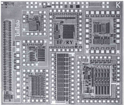
Joint project. This is one of the chips in the 1979 round-robin design project, which Lynn Conway calls a network adventure involving students in a multichip, multiuniversity project.
The MIT class marked a triumphant return there for Conway, who had studied physics at the school before transferring to Columbia. She had joined International Business Machines Corp. at its Yorktown Heights, N. Y., research headquarters in 1964, moving to California the next year when it established its advanced computer research laboratory in Menlo Park. While at IBM, she made major contributions to the architecture of ultrahigh-performance computing systems. In 1969 she joined Memorex Corp., where she was processor architect of a small business computer just before Memorex decided to get out of that market. She joined the Xerox research center in its early days in 1973 and began working on a combined optical character recognizer - facsimile system. It was that project that triggered her desire to create systems in VLSI.
Mead's interest in design automation goes back to the late 1960s, during a project to scale down ICs. "Calculations on how small they could go showed that the answer was lots smaller - down to 0.25 micrometer." Since at that time minimum feature dimensions were down only to 10 micrometers, Mead's conclusion itself was controversial. "But to this day the 0.25-micrometer figure has held up, despite many people taking cracks at it," he says.
Nevertheless, posing the possibility that geometries that small were within reach raised the central question of how to design them. "Since then we've been trying to find out," Mead says.
Along the road to that knowledge came Caltech's first algorithmic software package for CAD. It evolved from a program for designing printed circuit boards that Mead purchased in 1970 for $5,000 out of a special research and development fund. Mead's graduate students designed an experimental clock chip, making their own masks, which were run through Intel's fabrication line. "We bootlegged it through unofficially," says Mead, "although we told Robert Noyce [Intel's vice chairman] and Gordon Moore about it later."
Any discussion about the Mead-Conway methodology comes back to the book. "In electronics, a new wave comes through in bits and pieces," observes Conway. "Usually, after it has all evolved someone writes a book about it. What we decided to do was to write about it while it is still happening.
"Our method was to project ourselves ahead 10 years, and then write the book as though reflecting back upon a decade. Then we would let the people in the community critique it, and let the book itself become the focal point for the creation of methods."
With such a large body of interdisciplinary knowledge available, Mead and Conway bad to struggle with selection. "We had to figure out which knowledge was not needed," she says, "and come up with the simplest subset required to do any digital design." The pair decided that n-channel MOS was the ideal technology for their methodology and also decided to bypass Boolean logic gates as an intermediate step. Replacing them: simple fieldeffect transistor switches and such devices as stacks, barrel shifters, and functional blocks that are replicated to form larger subsystems. "We also decided that we could normalize the design rule-to the resolution of the process," says Conway. "Later on, we could ask about the value of the minimum line width."
By putting together a set of design rules that was independent of line width, Mead and Conway were avoiding some of the difficulties of standard semiconductor design practice. They skirted the issues of fine tuning of the fabrication line by making some fundamental assumptions about such questions as how wide metal should be in proportion to polysilicon. "We wanted to come up with something that students would learn once and retain," says Conway, "We chose the ratios based on Carver's knowledge of where the processes are headed." These ideas anchored the book.
Any lingering doubts about the practicality of Mead and Conway's approach must have been dispelled by the appearance of the Motorola 68000, the 16-bit microprocessor whose design was significantly influenced by the duo's methodology. The 32-bit iAPX-432 from Intel put the icing on the cake.
Besides the commercial-components that have benefited from Mead-Conway design rules, a complex experimental floating-point processor was designed by Digital Equipment Corp. using the duo's principles. The job took much less time than with traditional methods. Also notable among VLSI chips designed in academia is MIT's public-key encoding IC with its 40,000 transistors.
1981 Achievement Award
For their work in structuring the methodology of the design of very large scale, integrated circuits, summed up in the basic textbook on the subject, "Introduction to VLSI Systems," Carver Mead and Lynn Conway have been designated by the editors of Electronics as the recipients of the magazine's eighth Achievement Award. The efforts of Mead, the Gordon and Betty E. Moore professor of computer science and electrical engineering at the California Institute of Technology at Pasadena, and Conway, research fellow and manager of the VLSI system design area at Xerox Corp,'s Palo Alto Research Center in California, have begun to transform the thinking of semiconductor makers around the world.
Previous winners have been: in 1974, Gordon E. Moore, president of Intel Corp. for his overall accomplishments; in 1975, the four developers of integrated injection logic, Horst Berger and Siegfried Wiedmann of International Business Machines Corp. and Arie Slob and Cornelius Hart of Philips of the Netherlands; in 1976, Robert C. Dobkin of National Semiconductor Corp. for linear-circuit development; in 1977, Charles H. House of Hewlett-Packard Co. and B. J. Moore, president of Biomation Corp., for major instrumentation innovations; in 1978, Paul Richman, president of Standard Microsystems Corp., for advanced developments in MOS technology; in 1979, Andrew H. Bobeck of Bell Laboratories for his role in the invention of magnetic-bubble memories; and in 1980, Abe Offner, Jere D. Buckley, and David A. Markle for their development of the projection mask aligner at Perkin-Elmer Corp.