- Notes to readers:
This paper described an overall computer design
process based on multi-level simulation. The methods described
are of historical interest because they build on the ACS-1's
architectural and logic-level simulation capabilities to create
comprehensive design for a design process enabling error-checking
at each level of design and insurance of design consistency at
the various levels.
-
- This design process would likely have
been implemented at IBM had the ACS-1 gone into production. A
version of this paper was presented for Lynn (by others) at a
major internal IBM simulation conference in 1969 (after Lynn
had left IBM), and was well received and widely commented upon
at that conference. It is likely that this work had impact upon
later trends in computer CAD. This work also helped inspire Lynn's
later multi-level design methodology work in VLSI microelectronics.
-
- This page was created by scanning and
OCR'ing the original IBM-ACS internal paper. Page numbers correspond
to the original. See the following link for
a scanned PDF of the original paper.
(PDF)
-
- This paper has been officially declassified
by IBM, and Lynn Conway has been granted a
worldwide license
to distribute it for historical and academic purposes.
For more background
and context on this paper, refer to Lynn
Conway's ACS-Archive Front-Matter.
-
-
- August 6, 1968
Advanced Computing Systems
- Menlo Park, California
-
-
- Subject: The Computer Design Process: A Proposed Plan for
ACS
-
-
- References:
- 1. ACS AP #66-022, ACS Simulation Technique, D. P.
Rozenberg, L. Conway, R. H. Riekert, March 15, 1966.
- 2. ACS AP #67-115, MPM Timing Simulation, L. Conway,
August 25, 1967.
- 3.A Proposed Logic Simulation System, L. Conway, October
31, 1967.
- 4. System Simulation Program in ACS Engineering, P.
Shivdasani, April 24, 1968.
- 5.Proposal for a Design Procedure for the ACS System,
Uno R. Kodres, July 19, 1968 (memorandum to D. P. Rozenberg).
- 6.Preliminary Description of Traceback and Simulation
in ACS Fault Isolation, D. G. Keehn, August, 1968.
-
-
- Memorandum to: File
-
-
- [signature]
-
- L. Conway
LC:aw
-
CONTENTS
-
- 1-1 Introduction
2-1 The Overall Design Process
3-1 System Architecture
4-1 Logic Design and Engineering
5-1 Design and Process Automation
6-1 Maintenance
7-1 Conclusions
-
- 1-1
-
- INTRODUCTION
-
-
- For many years, computer designers have proposed the use
of various levels of simulation for design specification, verification
and evaluation. Simulation and automation have been applied to
some phases of the design process in a number of past projects.
-
- At the present time, in ACS, we feel that we have sufficient
practical experience in system simulation and design automation
to propose a workable system plan for the whole computer design
process.
-
- This plan has as its key element the specification of the
system level design in a high-level simulator. All following
phases of design are viewed as implementations of this system
specification.
-
- Details of this plan are presented including initial design
studies using timing simulation, design specification in a high-level
simulator, logic design verification by comparing two levels
of simulation, design automation and finally, hardware checkout
and maintenance.
-
- Design automation eliminates routine human effort in the
later design phases. Simulation allows creative human effort
where it is important -- in the initial system level planning
and evaluation. Rather than being merely a sideline in the design
process, simulation can be and should be viewed as the natural
medium of expression of the computer designer. A designer who
can quickly generate working models of his ideas can get the
feedback necessary for real design improvements. Adequate programming
tools are now available to the designer for this purpose.
-
- This memorandum presents a brief description of all the phases
and components of the design process as it might exist in ACS.
Much of this material is well established practice, and thus
the memorandum could serve as an introductory tutorial document
on this subject.
-
- The purpose of this memorandum is to make certain specific
suggestions concerning important aspects of the planning, implementation,
and operation of the total design process. The most important
of these suggestions are
-
- 1-2
-
- (i) The careful planning of the design process itself is
as necessary for success of the project as is the careful planning
of the computer design. The design process should be planned
as one integrated system. If the separate phases are planned
by different groups of people, the result will be an ineffective
overall plan with serious difficulties at the interfaces of the
phases.
-
- (ii) The plans produced should be carefully documented and
maintained and made available to all designers. A common terminology
would then develop for all the many design phases, simulation
and design auto-mation programs, design languages, etc., and
better understanding and communication would develop across design
group boundaries.
-
- (iii) It is strongly urged that the output of the Architecture
department be a formal, high-level description of the computer
in the form of a running simulator of
the system architecture. This simulator would have to be maintained
and modified as the design proceeded into later phases. This
simulator would, in effect, be the design of the machine with
all later phases viewed as implementations of the design. The,
use of a high-level language for this description is emphasized
to insure that the system description be readable and
intelligible to all designers. With the design formalized at
a high level the prediction of performance,
modification, debugging and general understanding of the design
would be greatly simplified and improved. Many of the essential
functions in the total design process proposed in this memorandum
are completely dependent upon the existence of this high-level
system architecture
- simulator.
-
- (iv) The design should be carefully "partitioned"
at the earliest possible point in the design process (i. e.,
in Architecture) into functional segments that will be manageable
by later design groups. Although it may be possible for a small
group of people to design and comprehend the entire computer
at the architectural level, it is not possible at later levels
of design. The computer must be divided or partitioned among
a number of groups of logic designers. If this partitioning is
done in architecture along functional lines, the interfaces between
partitions can be kept narrow and simple. These interfaces must
be formally specified
-
- 1-3
-
- in the high-level simulator and maintained throughout later
phases of design. The design process described in this memorandum,
including the above suggestions and the many programs implementing
the process, is not just a speculation as to what might be a
good way to do things in the distant future. There is considerable
practical experience within ACS with the various components of
the process.
-
-
- 2-1
-
- THE OVERALL DESIGN PROCESS
-
-
- Let us now identify and define the fundamental stages of
the overall design process. Then in the following sections of
the memorandum each stage will be described in some detail.
-
- The design and production of the computer passes through
four rather distinct stages. The stages are identified by their
final production of a "formal description" of the computer
in a particular "language". The output of one stage
is the input to the succeeding stage. Each stage of the process
may bethought of as implementing or redescribing the design of
the prior stage in a lower level language.
-
- These stages are as follows (see Figure 1 for a visualization
of the process):
-
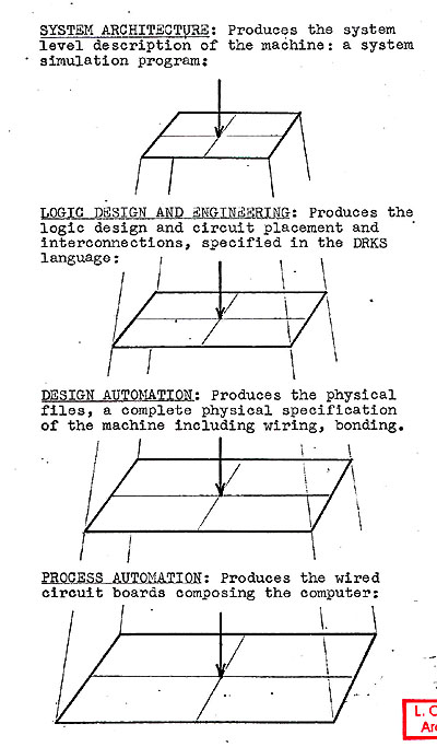
- System Architecture: This is the planning of the structure
and function of the computer system, developed from a consideration
of predicted market conditions and technology. The plan is developed
to the level of detail of system description such that the complete
function of the system is specified. The formal description produced
by the architecture group would be a running system level simulation
program written in a high-level language. The design would be
carefully partitioned along functional lines into formally specified
partitions with fairly narrow interfaces between them. The architectural
design would consist of (i) variables and arrays in the high-level
language symbolizing the various registers and control latches
of the machine, and (ii) algorithms in the language expressing
the functioning of the control latches and the flow of data between
registers and functional units on a cycle to cycle basis.
-
- Logic Design and Engineering: The logic designers
and engineers implement the structure and function of the architectural
design in the logic circuitry and physical package of the chosen
technology. The logic designer identifies and implements all
the latches specified in the architectural design and designs
combinational logic circuitry to connect the latches and implement
the algorithms of the architectural design. This logic design
must then be mapped onto real physical circuitry. This involves
the selection of a circuit chip on which a given logic circuit
is to be found, and the placement of that chip on a particular
MCM on a board. The interconnections between all such chips,
MCM's and boards must be specified. The output of
-
- 2-1a
-
- FIGURE 1: VISUALIZING THE STAGES OF THE COMPUTER DESIGN
PROCESS:
-
- Each stage produces a partitioned description of the machine
design in a formal language, Each stage implements the design
of the preceding stage. in a lower level language, with the design
then containing more detail but performing the same function.
The partitions can pass thru the process independantly.
-
-
-
- 2-2
-
- this design phase is a formal specification of the logic
design, placement, and interconnections in the input language
to the Design Record Keeping System (DRKS), which stores the
design in a set of computer files. An alternative logic description
language is now in development.
-
- Design Automation: In the design automation phase
a set of computer programs operate upon the design filed in DRKS
to produce as output a complete physical description of the computer.
This is done on a board by board basis. Note that in the DRKS
system the various pads which must be interconnected to form
a net are specified. However the actual route of wiring to connect
these points is not. This wiring of all the nets on a board is
computed by a wiring program. The pattern for bonding the wires
to the pads is completed, and terminating resistors are assigned.
The result of this design automation phase is a set of computer
files which contain the complete physical description of all
the boards of which the computer is composed.
-
- Process Automation: We now have a complete physical
description of all the boards. But how do we actually wire a
board; what sequence of wire placements should we make? We must
compute an orderly and feasible sequence of wire placements to
be made by wiring machinery. The process automation programs
operate on the physical files to produce a set of tapes which
drive the wiring machinery through the proper sequence of operations
to wire the boards of the computer. The output of this phase
is the physical computer itself.
-
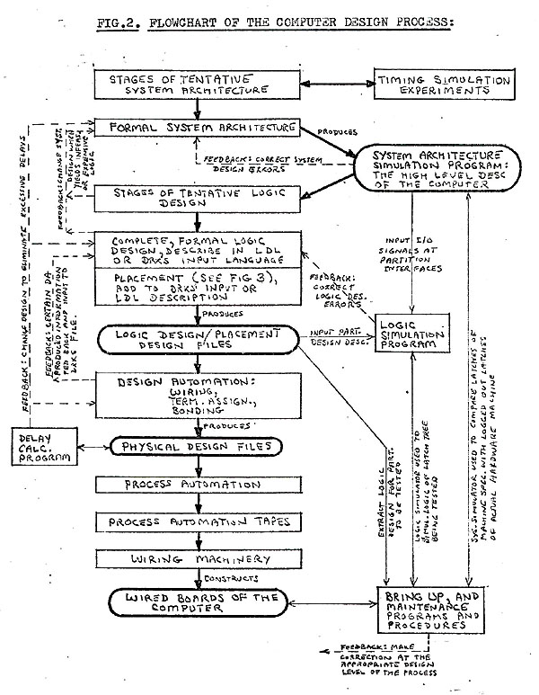
- We are now ready to study the design process in more detail.
Figure 2 is a flow chart of the stages of the design process
which indicates the various computer programs used at each stage
and the interaction of the various stages. This flow chart serves
as a basis for the detailed descriptions of each stage which
follow in the later sections of this memorandum.
-
- 2-2b
-
-
-
- 3-1
-
- SYSTEM ARCHITECTURE
-
-
- The function of the system architecture phase of design is
to produce a system-level specification of the machine. In the
design process as described in this memorandum this specification
is to be in the form of a running system simulation program.
-
- Tentative System Design: The development of a system
design which effectively meets cost and performance requirements
calls for considerable experimentation with tentative system
designs. The design will thus pass through these tentative, experimental
phases until the experiments
indicate that it is satisfactory. Then the design can be completely
placed into a formal description.
-
- Now, how can one experiment with a tentative computer design?
It turns out that this is well established in ACS --by using
a timing simulation program. See Reference 2 for a description
of a past timing simulation effort, and Reference 1 for the simulation
technique used in that effort.
-
- The timing simulator is written at essentially the same level
of description as the later system-level simulator and using
the same simulation technique. However, it can be simpler and
quicker to write because it does not require a data flow. Only
the timing of control operations is relevant to timing simulation.
The input to the timing simulator is the stream of instructions
to be processed by
the simulated computer, and the output of the simulator is a
chart of the activities in the various machine registers, initiated
by the instructions being processed, as a function of time. The
detailed model of the proposed control structure can thus be
tested quite accurately to predict performance and uncover design
bottlenecks.
-
- In order for timing simulation to really interact with and
affect the system design, the simulator must be running while
the system design is in development. This is only possible if
-
- (i) The system architects really want a simulator, believe
in its value, and help in its production.
-
- (ii) The timing simulator is written in a high-level language.
This will make algorithm production and documentation much easier
than would assembly coding. Also, the timing simulator would
be consistent with and a basis for the later system simulator.
3-2
-
- (iii) The architects participate in its writing.
-
- If the simulator writer(s) must form all the detailed algorithms
specifying a tentative design, then the simulator will lag the
design by many months, perhaps 4 to 6 months. However if the
architects specify their tentative design in detail, then the
coding of these designs would be a far simpler process and might
lag specification by only one or two months.
-
- This simulator should be partitioned along the same lines
as the machine and interfaces identified early in the design
processes. Then the separate partitions could be designed independently
with unspecified partitions modeled in the simulator by dummy
subroutines which roughly approximate the function of those partitions.
In this way the entire machine can be simulated as early as possible
even though some sections are not completely designed. Studies
can then be made on those sections which have been designed.
-
- Formal System Design: When timing simulation experiments
indicate that the system design is satisfactory and unlikely
to change greatly, the construction of a complete system simulator
describing that design can begin.
-
- The design will already have been partitioned. Engineers
from the logic design groups assigned to implement these partitions
could work along with the architects to write the system simulator.
This simulator must be carried uniformly to the latch level of
detail in order to be useful in later stages of design. The engineers
could see that this requirement is met and that all algorithms
specified for latch to latch operations in one cycle could probably
be implemented in combinatorial logic without breaking the machine
cycle.
-
- There is experience in ACS with this sort of simulation,
where a number of engineers write the program rather than having
a simulation programmer do it. See Reference 4.
-
- Note that this production of the system level design by both
architects and engineers blurs the traditional boundary between
the two functions. Both groups of designers work on the system
level design, but from different orientations.
-
- When the system description is complete, it can be run as
a simulator and the design debugged at this level by running
many actual programs on the "computer". As the later
stages of design are completed,
-
3-3
-
- much information will be fed back to the architectural stage
and force revisions in the system description. For example, many
algorithms will not turn out to be realizable in logic in one
cycle, and will have to be respecified, changing the system description.
This system description must be accurately maintained if the
design process as described in this memo is to function properly.
-
- The availability of an accurate, maintained system level
simulator will result in:
-
- (i)Accurate performance prediction- -potential users, compiler
writers, etc., can run code on this simulator and predict machine
performance and optimize their programs.
-
- (ii) The logic design of the machine will proceed directly
from the high-level description and thus will progress more rapidly
and with better communication between design groups working on
different partitions.
-
- (iii) An effective logic simulation can be performed to compare
the logic design of a partition with the system specification
of that partition. The system level simulator can produce the
input/output signals on the partition interface which can then
be used to "drive" the logic simulator. More will be
said about this very important logic simulation later in this
memorandum.
-
- (iv) Accurate system simulation plus accurate logic simulation
will make possible the implementation of a very effective maintenance
plan. This will be described later in this memo. See also Reference
6.
-
- The significance and importance of the system level simulator
cannot be overemphasized. It must be produced and maintained
for the proposed scheme to work. The higher the level at which
a design is formally specified, the easier it is for everyone
involved to fully understand the design, experiment with it,
and change and debug that design.
-
- This system level simulator should really be viewed as "the
machine". All later design and automation of design and
manufacture should be viewed as implementations of the system
design.
4-1
-
- LOGIC DESIGN AND ENGINEERING
-
-
- This stage of the design process produces an implementation
of the structure and function of the architectural design in
the logic circuitry and physical package of the chosen technology.
-
- In a manner similar to the system design, the logic design
and engineering pass through two phases: (i) a tentative phase
where attempts are made at implementation, often resulting in
revisions being made in the system design, and (ii) a formal
phase where the formal description of the logic and physical
placement is produced.
-
- Tentative Logic Design: When a partition of the system
has completed tentative system design and is ready to be formalized
in the system level simulator, then the tentative logic design
of that partition may begin. The tentative logic design is the
attempt at implementation of the system partition in logic circuitry
and package. These early attempts will fail because many of the
system algorithms will not be realizable in one machine cycle
of logic. A strong interaction must exist between those persons
producing the formal system specification and the logic designers.
The tentative logic design efforts must feed back enough information
such that the formal system description will have most of the
algorithms checked for feasibility of implementation in logic
and package without breaking the machine cycle time. For this
reason it is suggested that at least one of the logic designers
who works on the tentative logic design of a partition also work
along with the architect for that partition and participate in
the formation of the system level description. In this way the
partition of the system will not only reflect architectural requirements,
but will be implementable, as described, in logic.
-
- These early, tentative logic design and placement efforts
will probably be specified nonformally. The designs at this stage
are traditionally sketched out as logic circuit diagrams on "yellow
sheets". Rough. approximations of circuit placement can
be made, and then estimates of delays and circuit counts can
be generated. These estimates will be fed back, and perhaps modify
the system design and/or the logic design.
-
- 4-1a
-
-
-
- 4-2
-
- Formal Logic Design and Placement: When tentative
logic design studies have produced sufficient feedback to finalize
the system design, then the formal logic design and placement
can begin. The formal logic design must implement in logic circuitry
the function of the system design. The behavior of a partition
of the machine, as seen at its interfaces, must be the same at
both levels of design, system and logic.
-
- There are two aspects to this implementation of the system
design: the implementation of the system function in logic circuitry
and the mapping of that circuit design onto real hardware.
-
- Currently the logic design phase is done by the designer
with no computer assistance. The mapping of the logic design
onto hardware and the placement of the different levels of hardware
may be done in part, or perhaps entirely by computer programs.
-
- The mapping or partitioning of logic circuitry onto hardware
and the placement of levels of hardware involves the following
levels: logic circuitry maps onto circuit chips, circuit chips
are placed on MCM's, and MCM's are placed on the board.
-
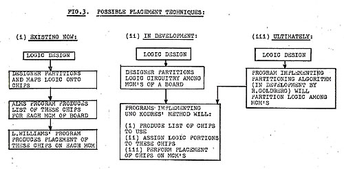
- There are a number of possible techniques that might be used
to accomplish the placement which involve varying amounts of
computer assistance to the designer. Some methods being considered
for ACS use are
-
- (i) In current use is a method where the designer must partition
the logic onto chips by hand, and then a sequence of computer
programs places the chips on MCM's on the board.
-
- (ii) In development is a placement system which will require
that the designer merely partition the logic among MCM's. The
selection of chips, assignment of logic to chips and placement
of chips on MCM's on the board would be accomplished by computer
programs. See Reference 5 which summarizes Dr. U. Kodres' work
in this area.
-
- (iii) It may eventually be possible to have the partitioning
of logic among MCM's be automated also, thus automating the entire
partitioning and placement process. Mr. R. Goldberg is working
on this partitioning algorithm. Also, Research has developed
a program, ALMS, which may be applicable.
- These three placement schemes are summarized in the flow
charts in Figure 3.
-
- 4-2a
-
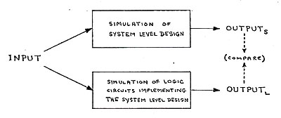
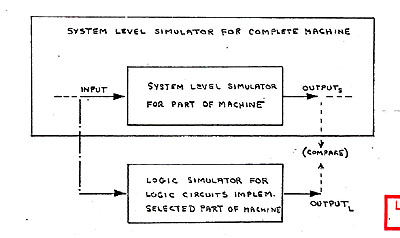
- Fig. 4. THE BASIC IDEA OF LSS: Apply the same input
to both levels of simulation and compare outputs. If outputs
are differenct then error exists in logic design:
-
-
-
- FIG.5. AUTOMATIC GENERATION FO SYSTEM LEVEL INPUT/OUTPUT,
LOGIC SIMULATOR INPUT: System level design is imbedded in
system level simulation of entire machine. When this simulator
runs, we automatically generate (and save) the I/O at the design
interface. We may later use these inputs to the logic simulator
for the same design and compare the logic outputs with the same
system level outputs:
-
-
-
- 4-3
-
- Formal Description of Logic Design/Placement: The
output of the formal logic design and placement is a formal description
of the design at this level. The language in which this description
may be placed is the DRKS input language. DRKS is the design
record keeping system which files the logic design and placement
information.
-
- An unfortunate aspect of the DRKS language is that it imposes
a totally arbitrary level of partitioning on the design description:
the ALD sheet (logic diagram sheet). The design is input to DRKS
by drawing logic diagrams on sheets of a fixed size and then
describing the drawing by statements in the DRKS language.
-
- This partitioning onto sheets is usually too fine to correspond
to any useful design partition. The designers partition of the
machine and even various functional entities within that partition
will contain logic circuitry requiring many, many ALD sheets
to describe. The language used to input DRKS is awkward to use,
and describes the sheets rather than the logic directly. The
statements of the language are usually formulated by someone
other than the designer, who merely sketches the sheets.
-
- It is strongly suggested that an alternative Logic Description
Language (LDL) be developed and used so that the designer can
more easily specify his logic design in a formal language. In
this way the processing and understanding of the logic designs
might be improved greatly. Dr. J. Cocke has proposed a tentative
version of such a language. Dr. R. Love, Mr. P. Shivdasani and
I are now working on completing the specification of this language.
-
- An important reason for the use of sheets as the formal logic
design description has been the traditional use of these sheets
by CE's who maintain the hardware. As we shall see later in this
memorandum (Section 6), the importance of the sheets may be reduced
because their use by CE's can be minimized by using improved
maintenance methods.
-
- If the ALD sheet were needed, perhaps in some central maintenance
facility, a form of ALD sheet could be generated by program from
the design files formed from LDL input. Thus there is no real
reason for requiring that the design be specified by sheets initially.
Another development which might really de-emphasize the importance
of ALD's is the possible use of prototype sheets. This plan involves
the use of a very limited total number of chip-types. Each chip
would be described by a prototype sheet. There would thus be
only a limited number of possible sheet types. These could be
stored as macros in a file. A design would be described by program
statements
-
- 4-4
-
- indicating the interconnection of such chips. No actual sheet
input would be necessary as the sheet would be implied by chip
type. Thus the logic could easily be described by a simple form
of LDL. Appropriate ALD sheets could be very easily generated
by program on those rare occasions
- when someone really needed to look at them.
-
- Logic Simulation: When the logic design of a partition
of the machine has been completed and formally described, it
is very desirable to verify that the logic design correctly implements
the architectural specification of the partition before going
any further into the design automation and process automation
phases. An error found at this stage will be much easier to correct
than if found later on.
-
- This verification of the logic design is performed using
a logic simulation program. A partition of the design can be
simulated on this program. Input signals are supplied at its
interface and the logic simulator produces the output signals
at the interface.
The major problem in this sort of logic simulation is the generation
of test cases of interface input signals and expected output
signals. The generation of a large enough set of such signals
to moderately debug a partition of logic would be a very costly
process if done manually. It would probably be possible to generate
only a rather small number of such tests.
-
- There is a solution to this problem. If the system level
simulator and logic description of a partition are really different
levels of description of the same entity, then they should behave
the same at the partition interface. Thus it would be possible
to run a program on the system level simulator and store all
the 1/0 signals on a partition's interface while the program
is running. Then these signals could be used to input and compare
against the logic of the partition when it runs on the logic
simulator. In this way many tests could be automatically generated.
The tests would be consistent over the whole machine; if we debugged
the logic of all partitions on a given program, then when we
put all partitions together later, they might all function properly
together when running that program.
-
- This idea of using two levels of simulation to debug the
logic design has been extensively studied and described in an
earlier memorandum. See Reference 3.
-
- Figures 4 and 5 graphically portray the idea of a Logic Simulation
System (LSS) using two simulators: a system simulator which provides
input/output signals for the partition which runs on a logic
simulator.
-
-
- 5-1
-
- DESIGN AND PROCESS AUTOMATION
-
-
- Suppose we now have a verified logic design along with physical
placement information resident in the DRKS files. There is still
a long way to go before the machine can actually be constructed.
The remainder of the design process is completely automated,
however.
The steps in the design automation process are as follows
(greatly simplified):
-
- (i)The records describing the logic design and placement
for a board are selected from the DRKS files.
-
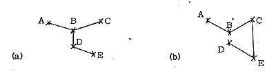
- (ii)The nets on the board must now be wired. This involves
determining the best path for wiring together the points of a
net subject to the wiring rule constraints. For example, given
that points A, B, C, D, E must be wired together we must decide
whether to wire as in (a), (b) or some other way.
-
-
-
- (iii) When the wiring has been calculated for the nets, we
must assign the location of terminating resistors for
the nets.
-
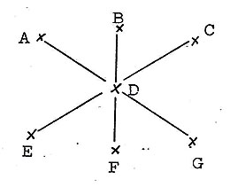
- (iv) Suppose we have wired A, B, C, D, E, F, G together as
follows:
-
-
-
- 5-2
-
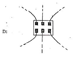
- We must now decide how to bond the wires on each pad of the
net. In the above example, D would be bonded as follows:
-
-
- The actual DA programming becomes somewhat involved because
a situation may arise in the later stages of processing which
cannot yield a solution, and this will have to be fed back to
the earlier phases and a new pass made through the DA programs.
-
-
- After the design automation is completed, we have in a "physical
file" the complete physical specification of the boards
of the machine.
-
- At this point we have sufficient information to perform delay
calculations to determine the circuit and wiring delays in various
paths through the machine. Computer programs can be written to
perform these calculations. Excessive delays will necessitate
design changes.. This raises an interesting point: We have proposed
four formal specification levels for the design. Thus, we can
envision four levels of design simulation: system, logic, "A-C"
logic including delays, and finally actual running hardware.
-
- Unfortunately, the "A-C" logic simulation, including
physical delays, is not really feasible for a machine of the
size we are designing. Even the usual logic simulation must be
partitioned, and the AC logic simulation includes much more detail.
So all we can do at this level is delay calculations on paths
through the hardware. It is of theoretical interest however to
note that with sufficient machine power a simulation at the physical
level could be performed and make this stage of the proposed
process similar to the preceding stages in the use of simulation
to verify the design.
-
-
- 5-3
-
- The phase in the design process which results in the production
of actual hardware is the process automation phase. After appropriate
reformatting, the information in the physical file describing
a board is input to the process automation programs. These programs
produce as output the tapes which drive the wiring machinery
which actually constructs the boards of the computer
.
Now, how can the boards (or MCM's) produced by the process automation
be debugged? Even if the design at the system level and logic
design level is error free, defects or errors may have been introduced
in the manufacture or wiring of the circuitry.
-
- It is possible to partially debug the hardware in an economical
manner by using the two levels of simulators to generate test
signals.
- The signals could be generated as follows: The system simulator
can produce input signals for the logic simulator while running
a particular program. This would be done for the logic simulation
of the partition of the machine which contains the hardware to
be tested (usually the hardware would be a small subset of a
partition). All of the signals internal to the partition are
generated during the logic simulation. Thus the signals at the
interface of the hardware to be tested could be extracted, and
filed, while running the logic simulator.
-
- Of course this method of debugging is only partial. Not all
possible input-output test patterns would be generated for the
hardware. However, this is a very special form of partial debugging:
the same program could be run on the system simulator to generate
tests for all hardware components. Thus, although only partially
debugged, the hardware will run that particular program when
it is all put together.
-
- The key point to note is that the partial debugging is uniform
over the whole machine. Of course many programs could be run
-- the number depending on the economics of the situation. Diagnostic
programs could be used for this hardware test generation. Then
the machine, when constructed, would run the diagnostics to isolate
residual hardware errors under normal maintenance procedures.
-
- Note that if each piece of hardware were very thoroughly,
but not completely, debugged with traditional methods, there
would be no assurance that any program would run when the pieces
were put together.
-
5-4
-
- Thus, the partial, but uniform, test generation could be
a very economical method of quickly getting hardware to the point
where it will run at least some programs when integrated into
the whole machine.
-
- This could serve as a basis for planning the bring-up of
the machine.
-
- 6-1
-
- MAINTENANCE
-
-
- The design process is not completed with the wiring and construction
of the computer. A bring-up of the computer must be accomplished
and the machine must be maintained. Bring-up may uncover design
errors at any of the stages of design. In addition to the correction
of hardware failures, maintenance will involve the installation
of engineering changes. Thus, both of these activities involve
cycling back through the design process and both are strongly
tied into the network of simulation and automation programs used
in the design process.
-
- At this time the bring-up process has not been completely
defined. However, a complete maintenance procedure has been defined
by Dr. D. G. Keehn (See Reference 6). This plan will be briefly
described here to indicate how it depends upon the simulation
programs. Some leads to ways of planning bring-up might be uncovered
in this maintenance plan. The scheme functions as follows:
-
- (a) Diagnostic programs running on the ACS computer detect
an error. The program causing the error is identified.
-
- (b) The error producing diagnostic- program is repeated on
both the ACS computer and on the system architecture simulator
running on a smaller diagnostic computer. The ACS computer's
latches are loaded out each cycle and compared to the latches
of the simulator. The failing latch and cycle of failure are
identified.
-
- (c) A traceback program is run on the diagnostic computer,
operating on the logic files, to find all latches which could
set/reset the failing latch in one cycle. This is the latch tree
of the failing latch.
-
- (d) All scopeable points in the logic of the selected latch
tree are found from the design files and output by another program
running on the diagnostic computer.
-
- (e) The logic of the latch tree is extracted from the design
files. A logic simulation of the latch tree is performed for
the cycles of interest: the cycle preceding failure and the failing
cycle. The scopeable point values are output for these cycles.
-
6-2
-
- (f) A technician can now scope the ACS machine at the appropriate
points and compare the values with the above values for the cycles
of interest. This will isolate the point of error.
-
- (g) The technician then decides what unit of hardware to
pull and replace in order to correct the failure.
-
- There are some very interesting operational characteristics
in this maintenance plan:
-
- (i) The diagnostic computer can be physically distant from
the ACS machine being repaired with communication between the
two locations handled by teleprocessing. Thus, one central diagnostic
computer and maintenance system could maintain several ACS machines
in the field.
-
- (ii) The person repairing the machine in the held need not
be a CE in the usual sense. He could be a technician instead,
for no knowledge of the functioning of computer logic would be
required to perform repair work.
-
- (iii) Because of (ii), it is clear that the distribution
of ALD sheets to many CE's in the field would not be necessary.
The significance of these sheets is thus greatly reduced.
- This particular maintenance plan has significant advantages
over previous plans. These advantages are bought at a price:
dependence on the existence of accurate system architecture and
logic simulators.
7-1
-
- CONCLUSIONS
-
-
- We have now covered all the phases of the design process
in some detail. For the sake of simplicity and brevity, the presentation
has treated these phases as separate activities which follow
each other in a serial manner.
-
- The actual design situation is obviously far more complex
and requires careful planning, scheduling and management of human
and machine resources. There are three factors in the process
(not fully developed in this initial memorandum) which lead to
this additional complexity:
-
- (i) Design phases do not follow serially, but overlap in
time. For example., the tentative logic design may be proceeding
while the formal system specification is still in process.
-
- (ii) There is a relative independence of the design of different
partitions. We might be far along in the design process on one
partition of the machine, but only experimenting at the system
level with another partition.
-
- (iii) There is consistent feedback (as indicated in Figure
2) from later phases of design to earlier phases. Very often
the design at a given phase cannot be feasibly or economically
implemented at a later stage and must be modified.
-
- Therefore this basic plan for the design process must be
made considerably more detailed and account for these additional
complexities before it is really a working plan for the process.
-
- This elaboration of the plan will have to await the feedback
produced by this memorandum.
-
- In conclusion, it is felt that the suggestions proposed in
this memorandum, especially the fundamental uses of the system
simulation program, can lead to a workable system plan for the
whole computer design process if they are properly elaborated
and detailed.
-
- A key factor in reaching this conclusion is the existence
of practical experience within ACS in the separate phases of
the plan.
-
- It is hoped that this memorandum will stimulate discussion
and new ideas on this subject. Your comments and criticisms concerning
the various suggestions made herein are welcomed by the author.
-
-
-
lynnconway.com >
ACS Archive front-matter > Design Process
-