
The CSIRO VLSI Research Program and AusMPC (cont.):
Photographs from 1982
Page compiled as part of Lynn Conway's VLSI Archive
[V 2-09-09]
During 1981, Dr. J. Craig Mudge founded a new VLSI Research Program at CSIRO (the Australian equivalent of NSF). The CSIRO program sponsored research in VLSI design and design tools, supported adoption of Mead-Conway methods and tools in Australian universities, and developed a national chip-prototyping infrastructure based on the MPC79 model to support the emerging chip design community there.
For more about the CSIRO program and the new national infrastructure, see the following paper:
"Australia's First Multi-Project Chip Implementation System", by J. C. Mudge and R. J. Clarke. (6p; 4.5mb PDF)
Photos from the first MPC operations of the program follow below:
1. Dr. J. Craig Mudge, head of CSIRO 's VLSI Program and Mr. Robert Clarke, who coordinated Australia's first Multi-Project Chip Implementation System. Designs submitted at the end of May were returned as packaged chips in mid-August - according to the forecasted 2 and 1/2- month schedule.
2. Technology transfer by CSIRO: Australia's first Multi-Project Chip (MPC) coordinated by the VLSI Program in Adelaide. Shown at the top is a circular silicon wafer (one of the seven steps in chip fabrication) containing many copies of the 46 Australian designs. In a later step in the MPC Implementation System, the wafer is diced, to produce the rectangular chips, which are then mounted in ceramic packages (one is shown below the wafer) for use in electronic equipment. The wafer fabrication was done in the U.S. in a $50 million plant; the packaging was done by an Australian firm, Philips Industries.
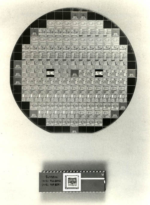
3. One of the seven steps in chip
fabrication: a circular silicon wafer containing many copies of the 46
Australian designs. In a later step in the MPC Implementation System, the wafer
is diced, to produce the rectangular chips, which are then mounted in ceramic
packages for use in electronic equipment. The wafer fabrication was done in the
U.S. in a $50 million plant; the packaging was-done-by-an-Australian firm,
Philips Industries.
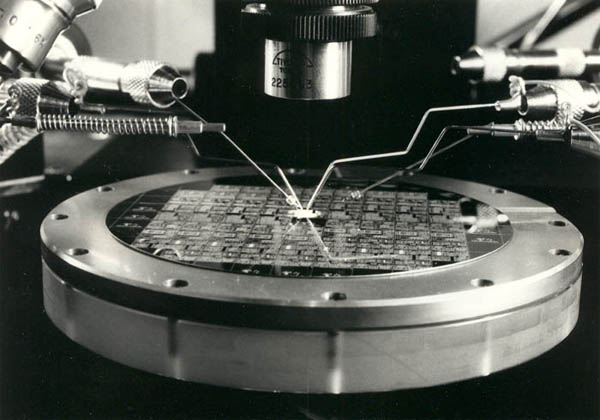
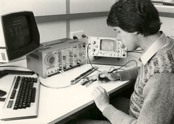
4. Micro-manipulating probes being used by CSIRO's VLSI Program to perform electrical measurements on Australian-designed silicon, before the dispatch of the chips to MPC designers across the country.
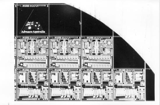
5. Several independent designs sharing a fabrication run. The design at top centre has been bonded (input-output connections wired). Other copies of the same chip would be bonded for the other designs. Forty-six different designs were fabricated on Australia's first Multi-Project Chip (MPC) Implementation System. Nearly 500 such chips were dispatched by CSIRO from its VLSI Program in Adelaide on17 August 1982.
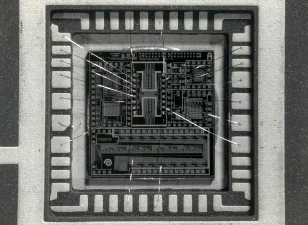
6. Engineer Ian Smith tests a silicon chip design done in Australian industry as part of a recent technology transfer achieved by CSIRO. This chip, designed by AMDEL (Australian Mineral Development Laboratories), for prototype fabrication on Australia's first Multi-Project Chip Implementation System, will be used in a new borehole logging probe.
7. A first-time chip designer, Mr.
Hugh McDermott_of the University of Melbourne, tests his custom chip for a
bionic ear for the 1990's. This innovative design is one of 46 end-user designed
custom chips fabricated on Australias first Multi-Project.Chip (MPC)
Implementation System organised by CSIRO in 1982.

LynnConway.com > Lynn Conway's VLSI Archive > VLSI Implementation Services > AusMPC > Photos